Materials & Technologies for Future Electronics
Materials & Technologies for Future Electronics
Led by Lain-Jong (Lance) Li
Materails Sciecne & Engineering National University of Singapore
Led by Lain-Jong (Lance) Li
Materails Sciecne & Engineering National University of Singapore
Materials Growth and Characterizations
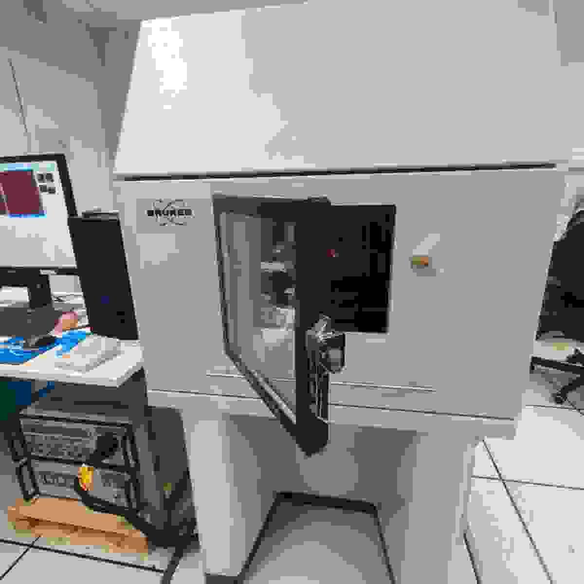
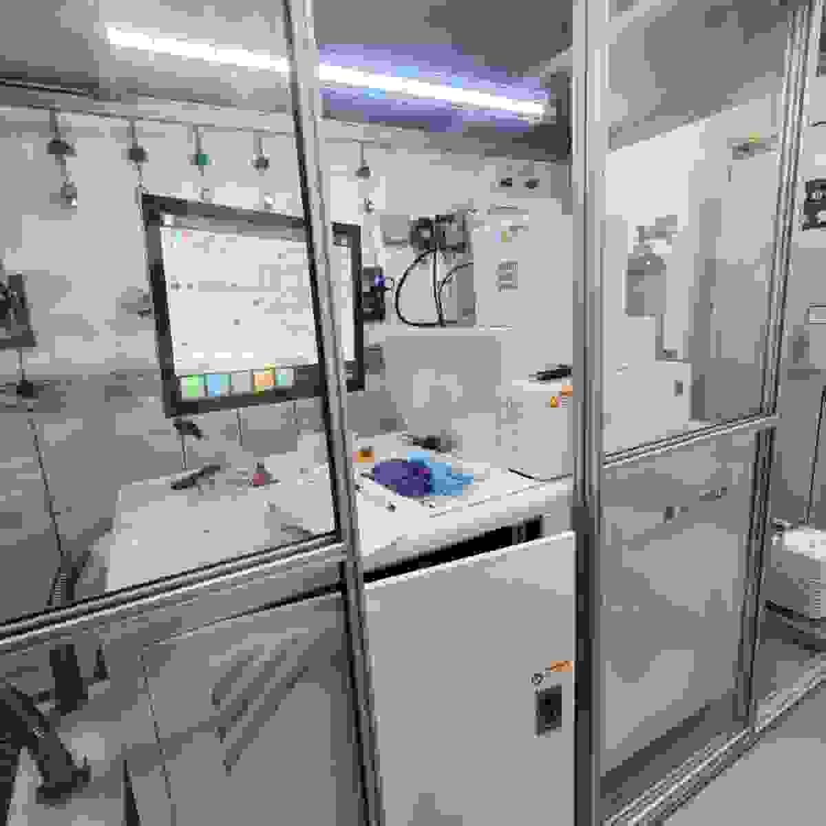
Furnace CVD for growing 2D layer semiconductors
We have at least 4 systems for growing different materials
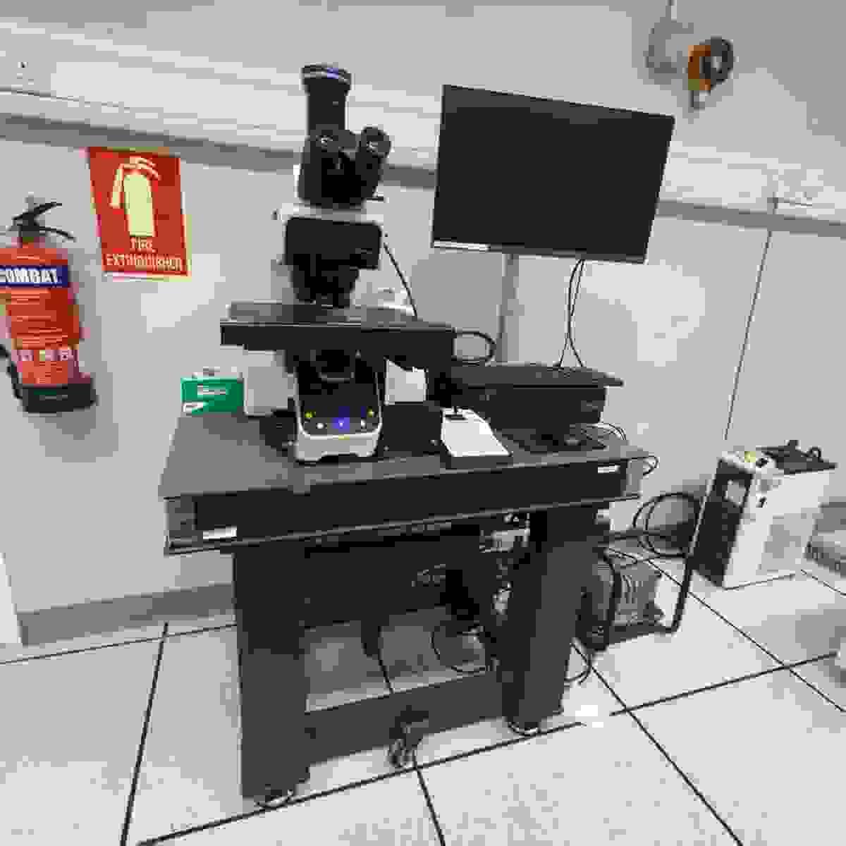
Confocal Raman spectroscopy
A high resolution Raman and PL mapping system, equipped with temperature control system
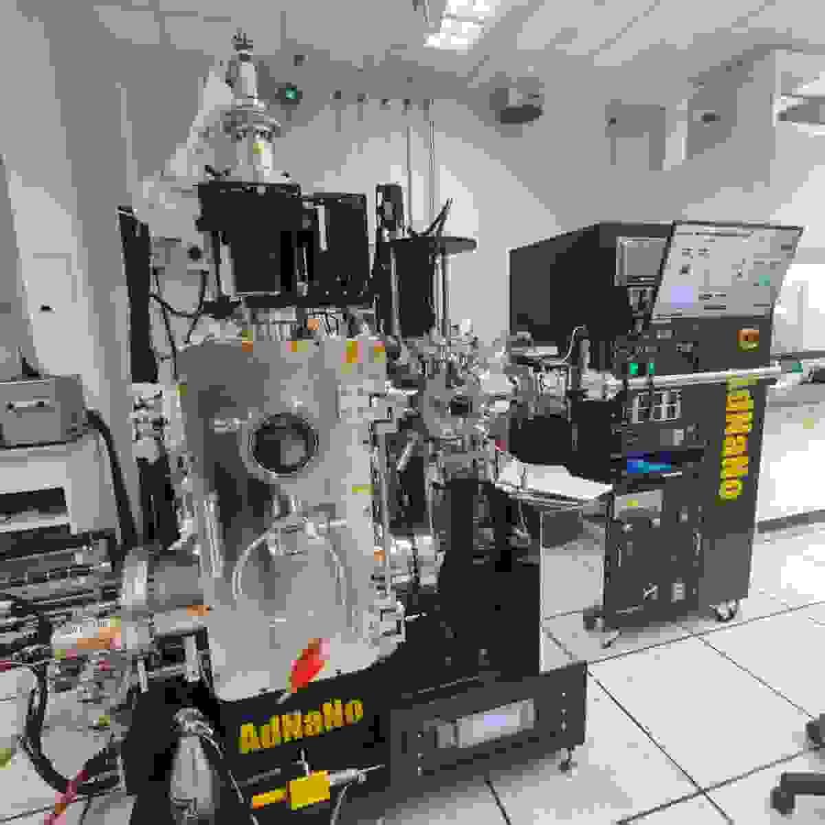
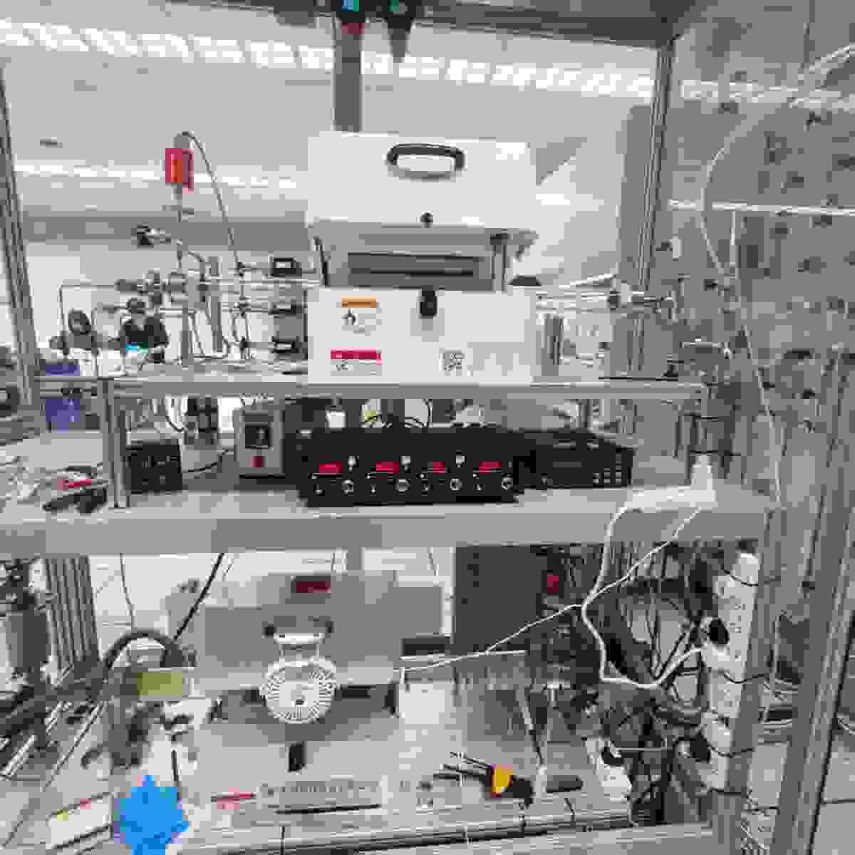
UHV thermal deposition for metals
Deposition of high-quality metals for high-performance devices
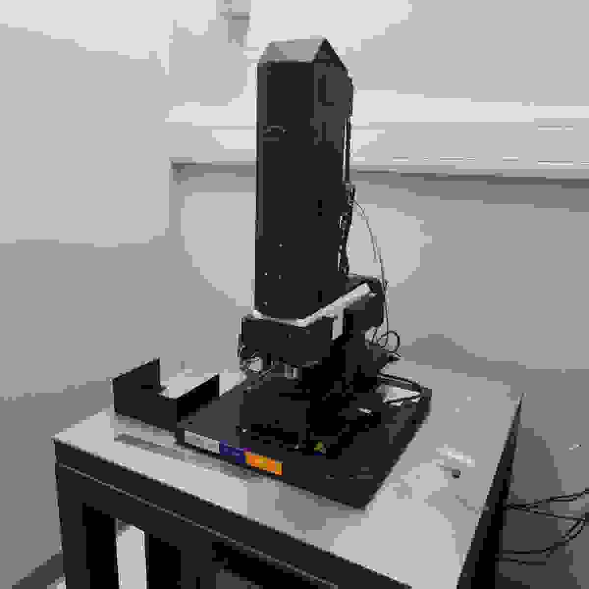
AFM
Topographic measurement for nanostructures
Optica Microscope
Examination of microscle features for devices
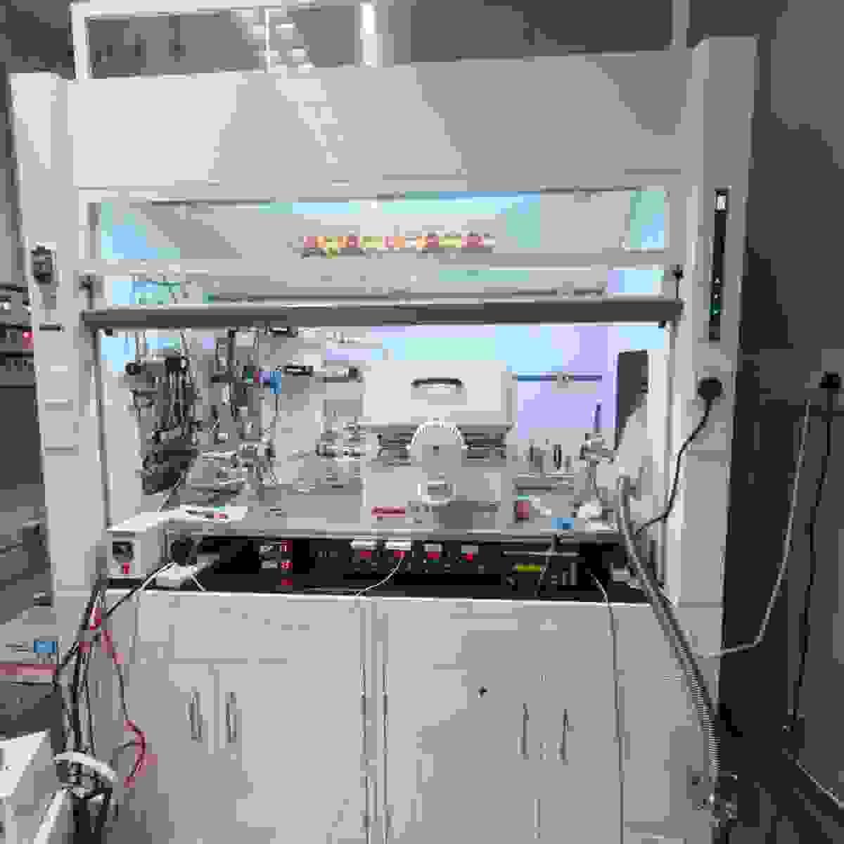
Thermal annealing systems for devices
Thermal annealing is used to enhance device performance
Device Fabrication and Measurements
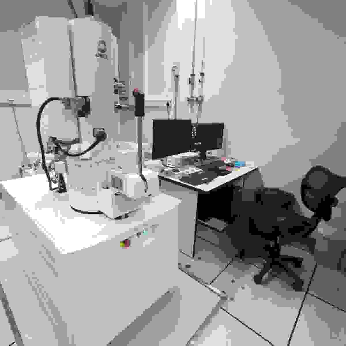
SEM/ EBL for imaging and patterning
Patterning of nanoscale devices

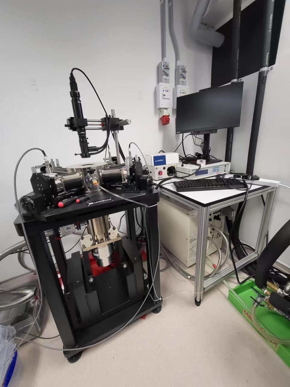
Cryogenic probe station
The system provides He close-cycle cooling environments for electrical measurements.
Atomic Layer Deposition
The system is adopted to develop new dielectrics materials